Year-wise Weightage (2016–2026)

YearQuestions AskedMarks
2026520
202528
2024312
2023624
2022312
Show earlier years (2016–2021)
2021312
202028
2019416
201828
201728
2016416
Q1
NEET 2016 Phase 2

What is the output Y in the following circuit, when all the three inputs A, B, C are first 0 and then 1?
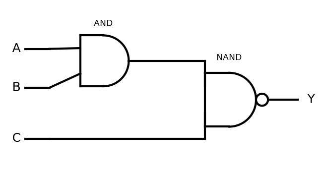
Semiconductor Electronics : Materials, Devices And Simple Circuits NEET PYQ diagram
Q2
NEET 2016 Phase 1

To get output 1 for the following circuit, the correct choice for the input is:
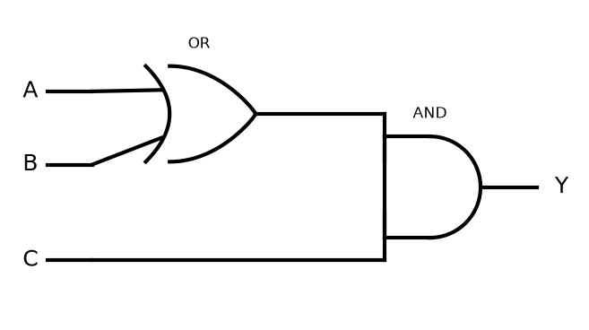
Semiconductor Electronics : Materials, Devices And Simple Circuits NEET PYQ diagram
Q3
NEET 2016 Phase 2

The given circuit has two ideal diodes connected as shown in the figure below. The current flowing through the resistance R₁ will be:
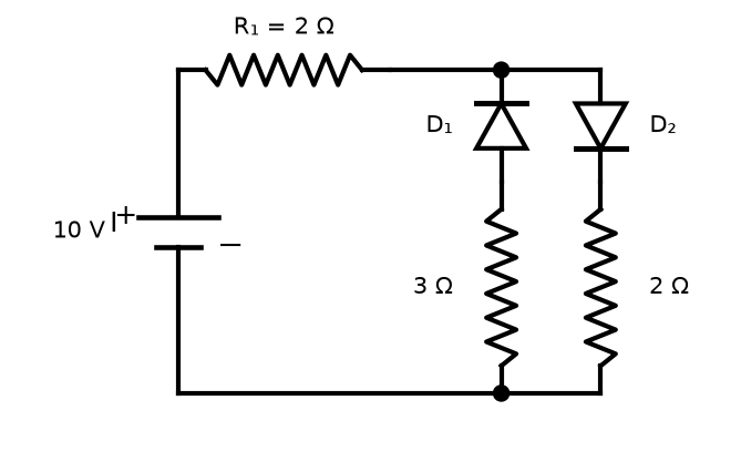
Semiconductor Electronics : Materials, Devices And Simple Circuits NEET PYQ diagram
Q4
NEET 2016 Phase 1

Consider the junction diode as ideal. The value of current flowing through AB is (refer to the given circuit):
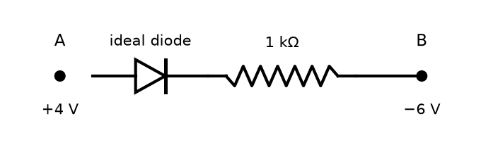
Semiconductor Electronics : Materials, Devices And Simple Circuits NEET PYQ diagram
Q5
NEET 2017

The given electrical network (with inputs A, B and output Y) is equivalent to:
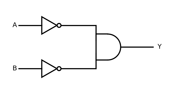
Semiconductor Electronics : Materials, Devices And Simple Circuits NEET PYQ diagram
Q6
NEET 2017

Which one of the following represents a forward biased diode?
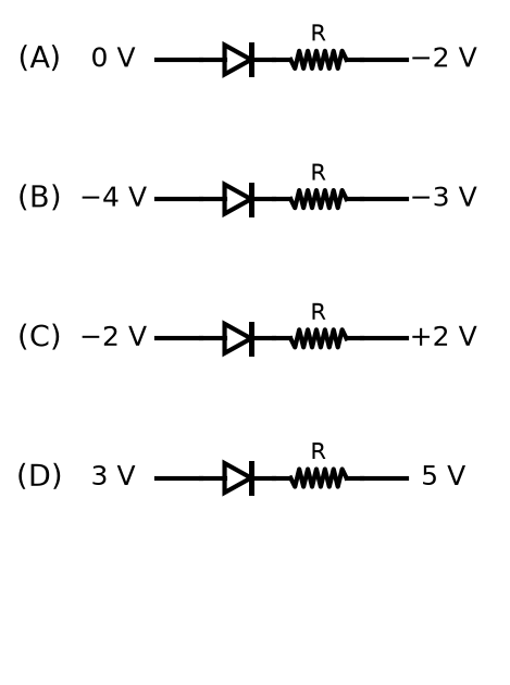
Semiconductor Electronics : Materials, Devices And Simple Circuits NEET PYQ diagram
Q7
NEET 2018

In a p-n junction diode, change in temperature due to heating:

Q8
NEET 2018

In the combination of the following gates, the output Y can be written in terms of inputs A and B as:
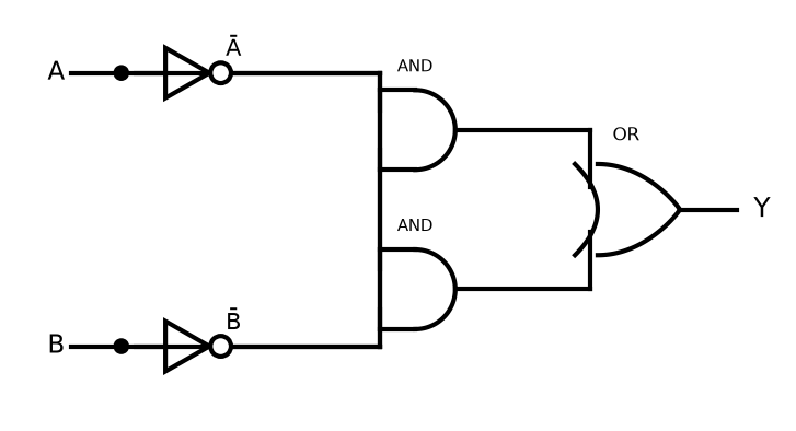
Semiconductor Electronics : Materials, Devices And Simple Circuits NEET PYQ diagram
Q9
NEET 2019

For a p-type semiconductor, which of the following statements is true?

Q10
NEET 2019 Odisha

The circuit diagram shown here corresponds to the logic gate:
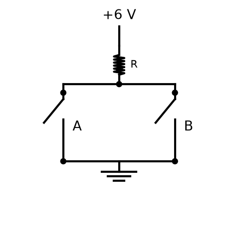
Semiconductor Electronics : Materials, Devices And Simple Circuits NEET PYQ diagram
Q11
NEET 2019 Odisha

An LED is constructed from a p-n junction diode using GaAsP. The energy gap is 1.9 eV. The wavelength of the light emitted will be equal to:

Q12
NEET 2019

The correct Boolean operation represented by the circuit diagram drawn (an LED Y driven from +6 V through resistor R with inputs A and B) is:
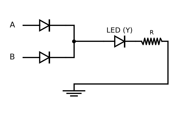
Semiconductor Electronics : Materials, Devices And Simple Circuits NEET PYQ diagram
Q13
NEET 2020

The solids which have the negative temperature coefficient of resistance are:

Q14
NEET 2020

The increase in the width of the depletion region in a p-n junction diode is due to:

Q15
NEET 2021

For the given circuit, the input digital signals are applied at the terminals A, B and C. What would be the output waveform at the terminal Y?
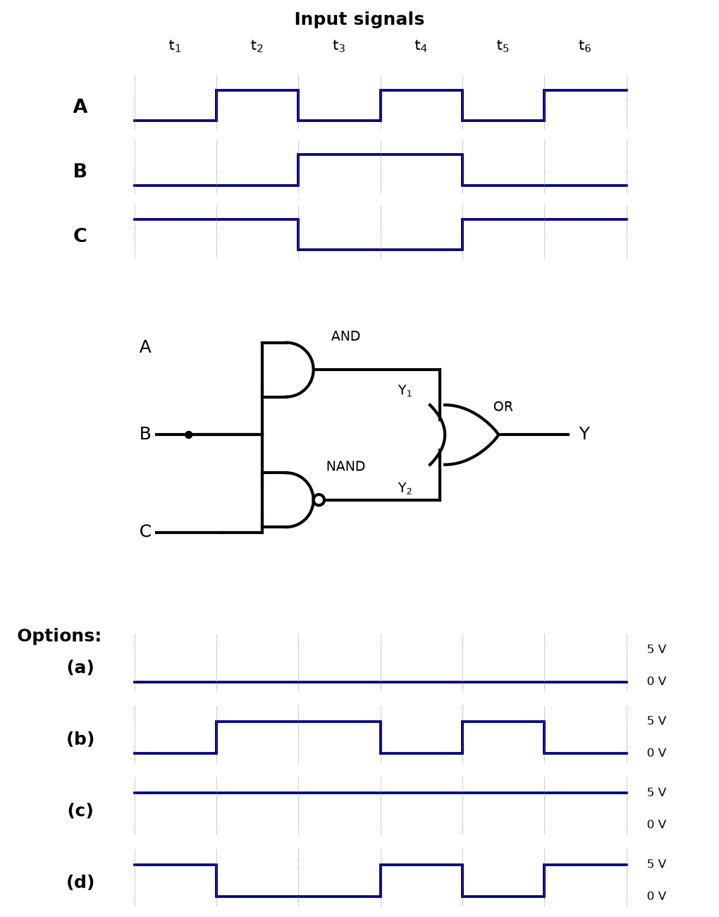
Semiconductor Electronics : Materials, Devices And Simple Circuits NEET PYQ diagram
Q16
NEET 2021

Consider the following Statements (A) and (B) and identify the correct answer. A. A zener diode is connected in reverse bias when used as a voltage regulator. B. The potential barrier of a p-n junction lies between 0.1 V to 0.3 V.

Q17
NEET 2021

The electron concentration in an n-type semiconductor is the same as the hole concentration in a p-type semiconductor. An external electric field is applied across each of them. Compare the currents in them.

Q18
NEET 2022

As the temperature increases, the electrical resistance:

Q19
NEET 2022

The truth table for the given logic circuit is:
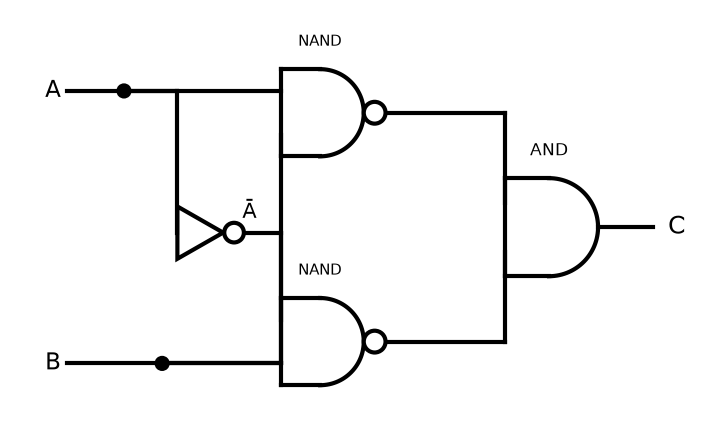
Semiconductor Electronics : Materials, Devices And Simple Circuits NEET PYQ diagram
Q20
NEET 2022

In half wave rectification, if the input frequency is 60 Hz, then the output frequency would be:

Q21
NEET 2023 Phase 2

On the basis of electrical conductivity, which one of the following materials has the smallest resistivity?

Q22
NEET 2023 Phase 1

For the following logic circuit, the truth table is:
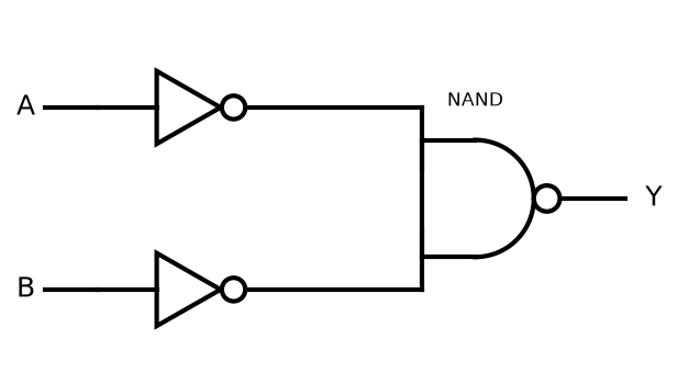
Semiconductor Electronics : Materials, Devices And Simple Circuits NEET PYQ diagram
Q23
NEET 2023 Phase 1

A full wave rectifier circuit consists of two p-n junction diodes, a centre-tapped transformer, capacitor and a load resistance. Which of these components removes the ac ripple from the rectified output?

Q24
NEET 2023 Phase 2

A p-type extrinsic semiconductor is obtained when Germanium is doped with:

Q25
NEET 2023 Phase 1

Given below are two statements: Statement I: Photovoltaic devices can convert optical radiation into electricity. Statement II: Zener diode is designed to operate under reverse bias in breakdown region. In the light of the above statements, choose the most appropriate answer from the options given below:

Q26
NEET 2023 Phase 2

The given circuit is equivalent to a single:
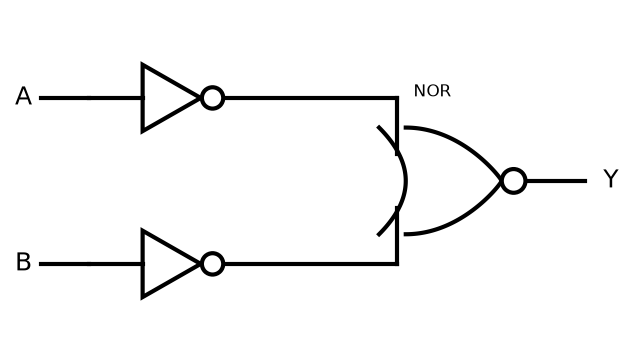
Semiconductor Electronics : Materials, Devices And Simple Circuits NEET PYQ diagram
Q27
NEET 2024

A logic circuit provides the output Y as per the following truth table: A B Y 0 0 1 0 1 0 1 0 1 1 1 0 The expression for the output Y is:

Q28
NEET 2024

Consider the following statements A and B and identify the correct answer: A. For a solar cell, the I-V characteristic lies in the IV (fourth) quadrant of the given graph. B. In a reverse biased p-n junction diode, the current measured in μA is due to majority charge carriers.
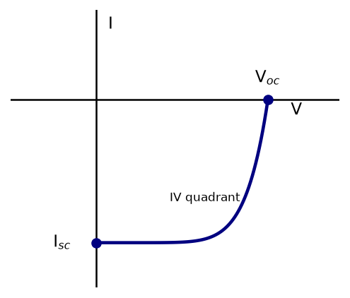
Semiconductor Electronics : Materials, Devices And Simple Circuits NEET PYQ diagram
Q29
NEET 2024

The output (Y) of the given logic gate is similar to the output of an/a:
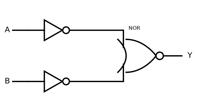
Semiconductor Electronics : Materials, Devices And Simple Circuits NEET PYQ diagram
Q30
NEET 2025

A full wave rectifier circuit with diodes D₁ and D₂ is shown in the figure. If the input supply voltage is V_in = 220 sin(100πt) volt, then at t = 15 ms:
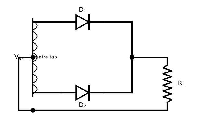
Semiconductor Electronics : Materials, Devices And Simple Circuits NEET PYQ diagram
Q31
NEET 2025

The output (Y) of the given logic implementation is similar to the output of an/a ____ gate.
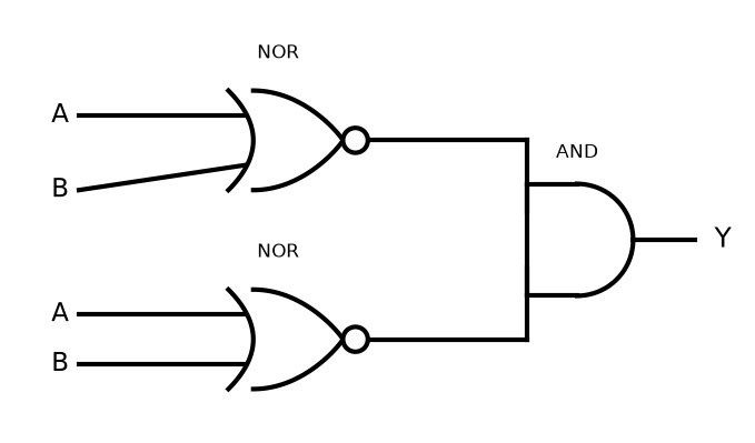
Semiconductor Electronics : Materials, Devices And Simple Circuits NEET PYQ diagram
Q32
NEET 2026 (1)

Two statements are given below: A. When the forward bias voltage across a p-n junction diode increases above a certain threshold voltage, the diode current increases significantly. B. This current is called reverse saturation current. Choose the correct answer from the options given below:

Q33
ReNEET 2026

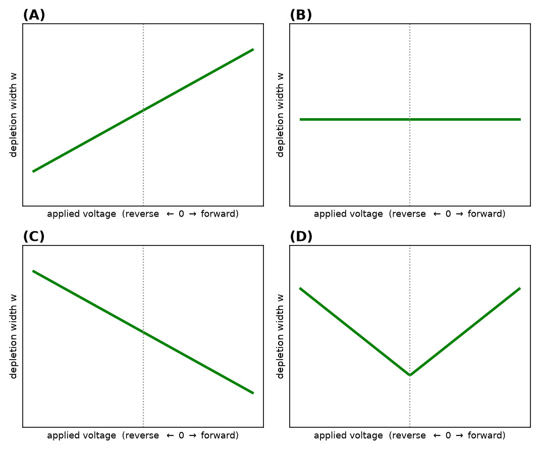
Three identical p-n junction diodes $D_1$, $D_2$ and $D_3$ are connected across a battery as shown (each in series with a $1\,$k$\Omega$ resistor). If the widths of the depletion regions of $D_1$, $D_2$, $D_3$ are $W_1$, $W_2$, $W_3$ respectively, then the correct option is:
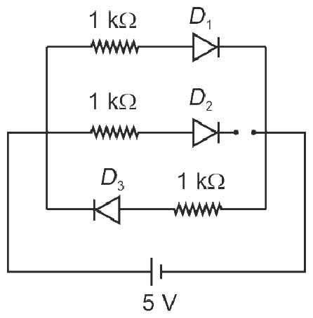
Semiconductor Electronics : Materials, Devices And Simple Circuits NEET PYQ diagram
Q34
NEET 2026 (1)

In the circuit shown below (an a.c. source in series with a diode D and a resistor R), the voltage appearing across the diode D will be of the form:
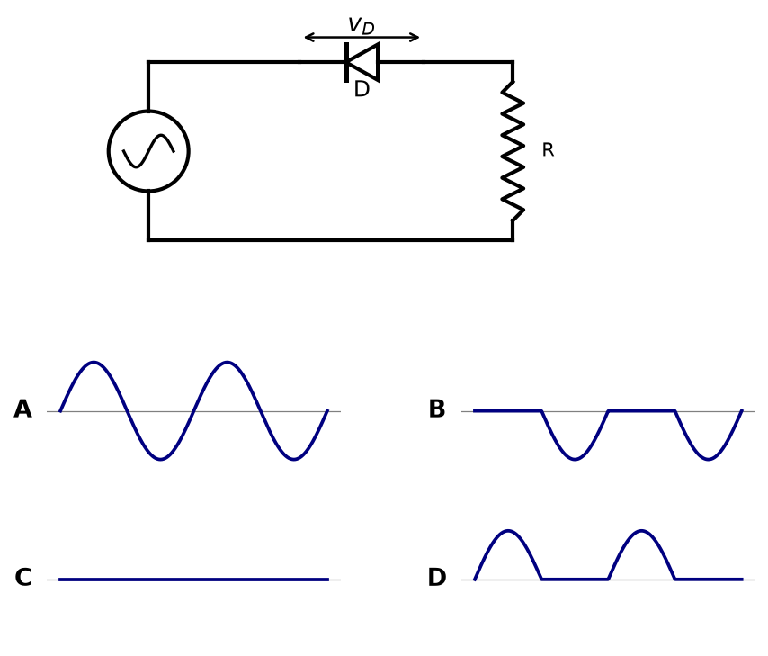
Semiconductor Electronics : Materials, Devices And Simple Circuits NEET PYQ diagram
Q35
ReNEET 2026

An ideal Zener diode with breakdown voltage of $-3\,$V is reverse biased with a negative input voltage $V_i=-5\,$V. In the circuit shown ($C$–[Zener]–$B$–$R$–$A$), the magnitude of the voltage difference between points $B$ and $A$ is:
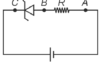
Semiconductor Electronics : Materials, Devices And Simple Circuits NEET PYQ diagram
Q36
NEET 2026 (1)

The current I in the circuit shown below is: (All diodes are ideal and identical)
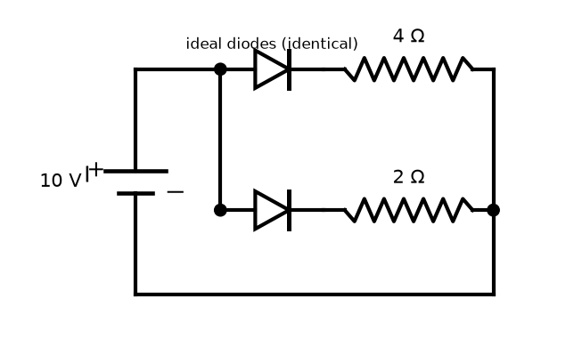
Semiconductor Electronics : Materials, Devices And Simple Circuits NEET PYQ diagram

Want more Semiconductor Electronics : Materials, Devices And Simple Circuits questions?

MedicNEET has 14,000+ NEET-style Biology questions with detailed NCERT-based explanations — including long, tricky questions that actually come in the exam.

Download MedicNEET App — Free
Practise Semiconductor Electronics : Materials, Devices And Simple Circuits MCQs — Free

Beyond the PYQs above — every Physics question format NEET now uses, starting with the newest ReNEET 2026-style reasoning MCQs. Tap an option for the answer and a worked solution. Free, no login.

🔢 Semiconductor Electronics : Materials, Devices And Simple CircuitsNumericals — PYQ-Based

Exam-style numericals seeded from real NEET previous-year questions, kept inside the NEET syllabus boundary. Each with a worked solution.

  1. Q1. A light emitting diode (LED) is fabricated from a semiconductor of band gap 2.0 eV. The wavelength of the light it emits is approximately (take hc = 1240 eV·nm):
  2. Q2. A p-n junction diode is connected in a circuit with a battery and resistor. The p-side is connected to the negative terminal of a 6V battery through a 300Ω resistor, and the n-side is connected to the positive terminal. Assuming the diode is ideal (zero forward resistance and infinite reverse resistance), what is the current through the circuit?
  3. Q3. A silicon p-n junction diode has acceptor concentration N_A = 10¹⁶ cm⁻³ on the p-side and donor concentration N_D = 10¹⁸ cm⁻³ on the n-side. At thermal equilibrium (300 K), the depletion region extends x_p into the p-side and x_n into the n-side. Which of the following relationships is correct?
  4. Q4. A p-n junction diode with built-in potential V₀ = 0.7 V is forward biased with an external voltage of 0.5 V. What is the effective barrier height that the charge carriers must overcome to cross the junction?
  5. Q5. A complex logic circuit is designed using universal gates. The circuit has three stages: First stage has two NAND gates receiving inputs (A,B) and (C,D) respectively. Second stage has a NOR gate receiving outputs from both first-stage NAND gates. Third stage has a NOT gate receiving output from the NOR gate. If A=1, B=1, C=0, D=1, and the final output is used to control a transistor that switches ON when output is HIGH, what is the final output Y and the state of the transistor?
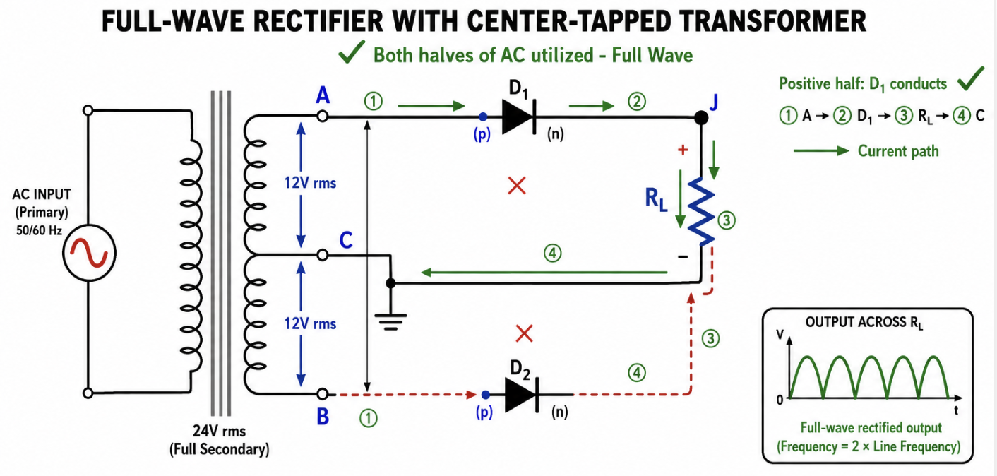
  6. Q6. In a full-wave rectifier circuit using two diodes D₁ and D₂ with a center-tapped transformer, the secondary coil provides 24V rms across the full secondary. If at a particular instant, terminal A is at +12V with respect to the center tap, what is the voltage at terminal B with respect to the center tap, and which diode conducts?
    NEET question diagram
  7. Q7. A silicon p-n junction diode has a built-in potential barrier V₀ = 0.7 V at room temperature. When a forward bias voltage of 0.5 V is applied, what is the effective barrier potential that charge carriers must overcome to cross the junction?
  8. Q8. A p-n junction diode has a built-in barrier potential V₀ = 0.7 V at 300 K. When a forward bias of 0.5 V is applied, the depletion region width reduces to W₁. When the forward bias is increased to 0.65 V, the width becomes W₂. A student then applies a reverse bias of 0.3 V and measures width W₃. If the depletion width under zero bias is W₀, and assuming the width varies as W ∝ √(V₀ - V) for forward bias and W ∝ √(V₀ + V) for reverse bias, what is the ratio W₁ : W₂ : W₃?
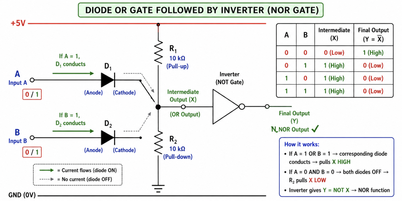
  9. Q9. A logic circuit is constructed using two diodes D₁ and D₂, two resistors, and connected to inputs A and B as shown. When both inputs are at 0V (logic 0), the output is at 0V. When either or both inputs are at +5V (logic 1), the output is at +5V. An inverter (NOT gate) is then connected to this output. The final output corresponds to which logic gate?
    NEET question diagram
  10. Q10. Three logic gates are connected as shown in the circuit. The inputs A and B are fed to an OR gate, whose output is then fed to a NOT gate, and finally this output is combined with input C through an AND gate. What is the final output Y of this logic circuit?

You’ve practised 10 of 60 Semiconductor Electronics : Materials, Devices And Simple Circuits questions in this set.

Practise all 60 + every chapter — free app →

📘 Semiconductor Electronics : Materials, Devices And Simple CircuitsConceptual Theory MCQs

Theory MCQs — assertion-reason, statement and standard — for the part of the physics paper that isn't numericals.

  1. Q1. At absolute zero temperature (T = 0 K), an intrinsic semiconductor behaves as a perfect insulator. According to the energy band theory, what is the primary reason for this?
  2. Q2. A solid material has an electrical resistivity of approximately 10³ Ω m. Based on this value, how is this material most accurately classified?
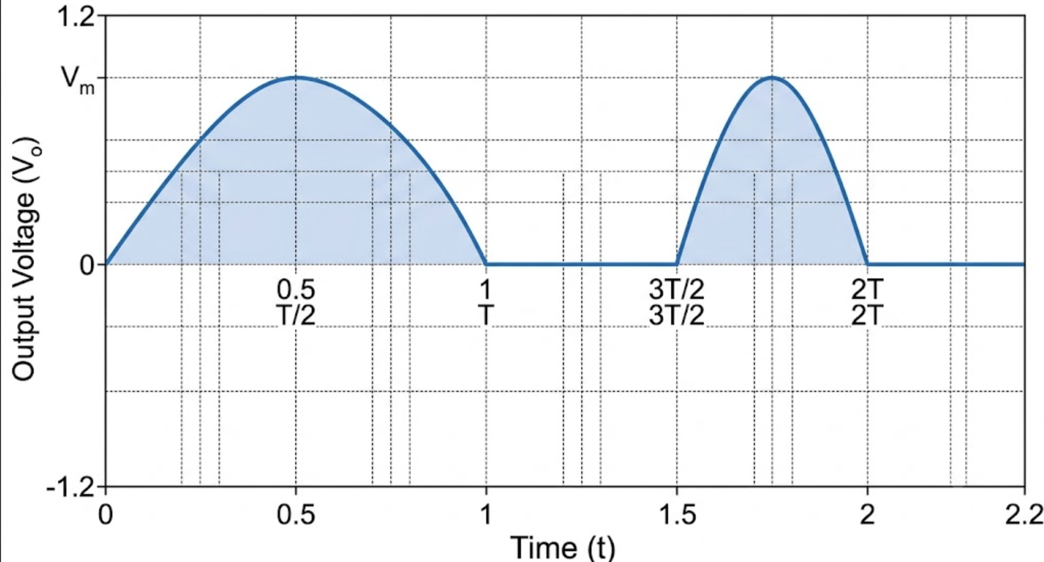
  3. Q3. The graph shows the output voltage () across a load resistor as a function of time () for a particular electronic circuit. What does this waveform represent?
    NEET question diagram
  4. Q4. A p-n junction is formed at the interface of p-type and n-type semiconductors. The space-charge region that forms on either side of the junction is also called the depletion region. What is the primary reason for this name?
  5. Q5. Match Column I with Column II. | Column I | Column II | |-------------------------------------------------------|------------------------------------| | (a) Elemental semiconductor | (i) Anthracene | | (b) Inorganic compound semiconductor | (ii) Silicon (Si) | | (c) Organic semiconductor | (iii) Polyaniline | | (d) Organic polymer semiconductor | (iv) Gallium Arsenide (GaAs) |
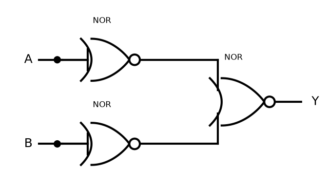
  6. Q6. In the circuit shown, both inputs of a first NOR gate are connected together to input A, and both inputs of a second NOR gate are connected together to input B. The outputs of these two NOR gates are then connected to the two inputs of a third NOR gate whose output is Y. The single gate equivalent to this whole network is:
    NEET question diagram
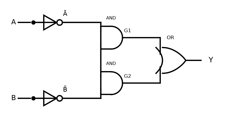
  7. Q7. In the network shown, A and B are each inverted to give Ā and B̄. One AND gate forms G1 = A · B̄ and a second AND gate forms G2 = Ā · B. The outputs G1 and G2 are fed to an OR gate giving output Y. The output Y and the equivalent gate are:
    NEET question diagram
  8. Q8. Which of the following correctly describes a light emitting diode (LED)?
  9. Q9. The output of a full-wave rectifier is a pulsating unidirectional voltage. To get a steady DC voltage, a capacitor is connected across the output terminals. Which one of the following graphs correctly represents the output voltage waveform across the capacitor filter?
    NEET question diagram
  10. Q10. The output Y of the logic circuit shown follows the truth table below: A B Y 0 0 0 0 1 1 1 0 1 1 1 1 The Boolean expression / equivalent single gate for Y is:
    NEET question diagram

You’ve practised 10 of 34 Semiconductor Electronics : Materials, Devices And Simple Circuits questions in this set.

Practise all 34 + every chapter — free app →

Semiconductor Electronics : Materials, Devices And Simple Circuits — NEET PYQ Analysis

Semiconductor Electronics : Materials, Devices And Simple Circuits is a Class 12 NEET Physics chapter consistently tested from 2016 to ReNEET 2026. This page has all 36 authentic previous year questions from real NEET papers — with answers and detailed solutions, not model questions.

For full chapter-wise practice in timed test mode, download the MedicNEET app — 22,000+ questions across the full NEET syllabus. Back to the NEET Physics PYQ index.